PCB trace
From HwB
According to recommendations in IPC-2221 (formerly IPC-D-275, MIL-STD-275) on how to calculate minimum PCB (printer circuit board) trace width.
Below table is valid for:
- PCB material FR-4
- Board thickness=1.6mm (0.063")
- Trace thickness=35µm (1 oz)
- Allowed temperature rise=10 °C
Contents |
Table
| Current | Width (inner) | Width (outer) |
|---|---|---|
| A | mils | mils |
| 0.01 | 0.308 | 0.118 |
| 0.05 | 1.54 | 0.591 |
| 0.1 | 3.08 | 1.18 |
| 0.2 | 6.15 | 2.37 |
| 0.4 | 12.3 | 4.73 |
| 0.4 | 12.3 | 4.73 |
| 0.5 | 15.4 | 5.91 |
| 0.6 | 18.5 | 7.1 |
| 0.7 | 21.5 | 8.28 |
| 0.8 | 24.6 | 9.46 |
| 0.9 | 27.7 | 10.6 |
| 1.0 | 30.8 | 11.8 |
Note: 1 mil = 1/1000" = 0.0254 mm
Graph
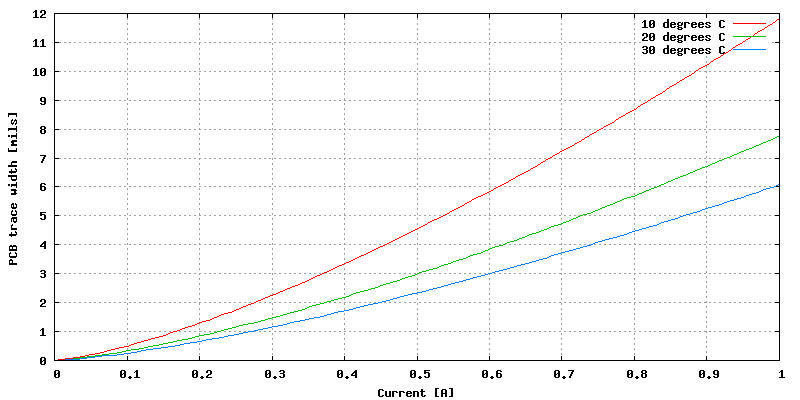
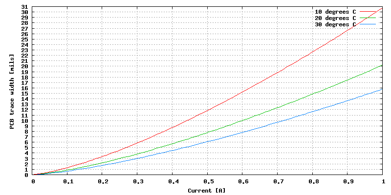
Outer traces (0-1 A)
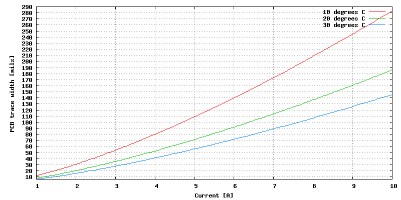
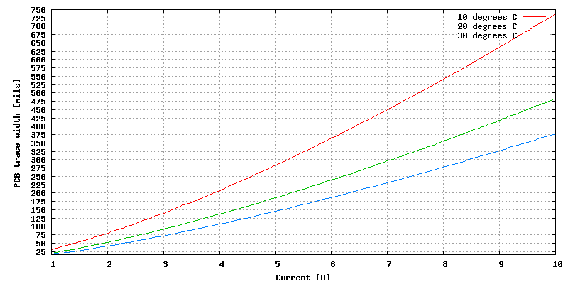
Outer traces (1-10 A)
Inner traces (0-1 A)
Inner traces (1-10 A)
Formula
Given:
- I [A] (Current)
- T [°C] (Temperature rise)
- m [oz] (Mass of PCB trace)
Constants:
- y = 1.378 [mils/oz] for copper
- b = 0.44
- c = 0.725
- k = 0.048 (for outer layers)
- k = 0.024 (for inner layers)
Formulas:
- A [mils²] = <math>{(\frac {I}Template:KT^b)}^{\frac {1}{c}}</math> (PCB trace area)
- l [mils] = <math>\frac {A}{m y}</math> (PCB trace width)
Links
- UltraCAD article: Current Carrying Capacity of Vias
- PCB Trace Width Calculator by Brad Suppanz
- New Correlations Between Electrical Current and Temperature Rise in PCB Traces by Johannes Adam at Flomerics Ltd.